
IC Design
Low-Noise Amplifier (LNA)
The purpose of LNA is to amplify weak RF signals without adding too much noise to them. An LNA is essential to every RF receiver. It is the interface of the circuit to the antenna. There are fours metrics to evaluate its performance: input impedance, noise figure (NF), voltage gain, and power consumption.
The input impedance of an LNA depends on its topology. Take a common-gate LNA as an example. Its input impedance is inversely proportional to the transconductance, , of the common-gate transistor. Given a certain transconductance efficiency, , this means the input impedance is inversely proportional to current consumption, or rather power consumption. To achieve low power consumption, the input impedance of the LNA has been designed to be
The sensitivity of the receiver can be derived as
, where BW is the bandwidth of the IF filter (200kHz in our design), NF is the noise figure of the receiver, and is the signal-to-noise ratio required by the backend circuits to demodulate the FM signal. The LNA's NF is inversely proportional to its power consumption. For an FM radio, there is no strict requirement on NF. But to compete with commercial FM receiver with the sensitivity of -110dBm, the NF of the LNA is designed to be 5dB and the NF of the system is designed to be 12dB. Then the sensitivity of our system is calculated as below, where we estimate to be 15dB.
The voltage gain of the LNA is designed to be 17dB. Along with 6dB passive gain from the matching network, there is 23dB gain from the antenna to the output of the LNA. To achieve a low power consumption and a high
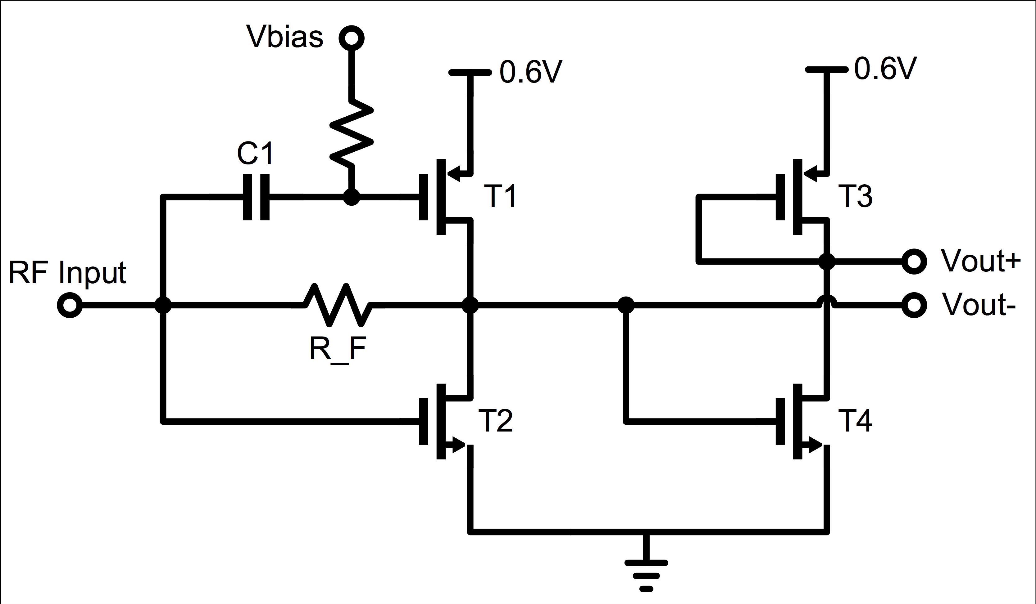
Fig.1 Simplified Schematic of LNA
Transistors T1 and T2 in Fig.1 form an inverter. A
AC simulations have been performed and show that the voltage gain is larger than 23dB from 88MHz to 108MHz.The input impedance, , can be expressed as
A S-parameter simulation has been performed and S11 is always below -10dB across FM frequency band.The NF can be expressed as
The simulation results show that NF is below 6.5dB across FM band.
Double-Balanced Mixer
Mixers are used to convert high-frequency RF signals to lower intermediate-frequencies (IF) for later signal processing. A typical IF frequency for FM radios is 10.7MHz since it offers a good image rejection with an 88MHz-108MHz band-selection filter. A number of off-the-shelf narrow-band IF filters are available at this frequency. There are three frequently-used metrics to evaluate the performance of mixers: conversion voltage gain, noise figure, and power consumption.
Double-balanced mixers have no LO or RF feed-through, compared to single-balanced mixers. Therefore there is less spurious response at IF frequencies. The requirements for IF filters are also alleviated. To lower power consumption, a low supply voltage of 0.6V is used in our design. Therefore, a switching-gm mixer [4] is chosen over Gilbert-cell structures. Current reuse structures are employed to provide higher conversion gain. The simplified schematic is shown in Fig.2.
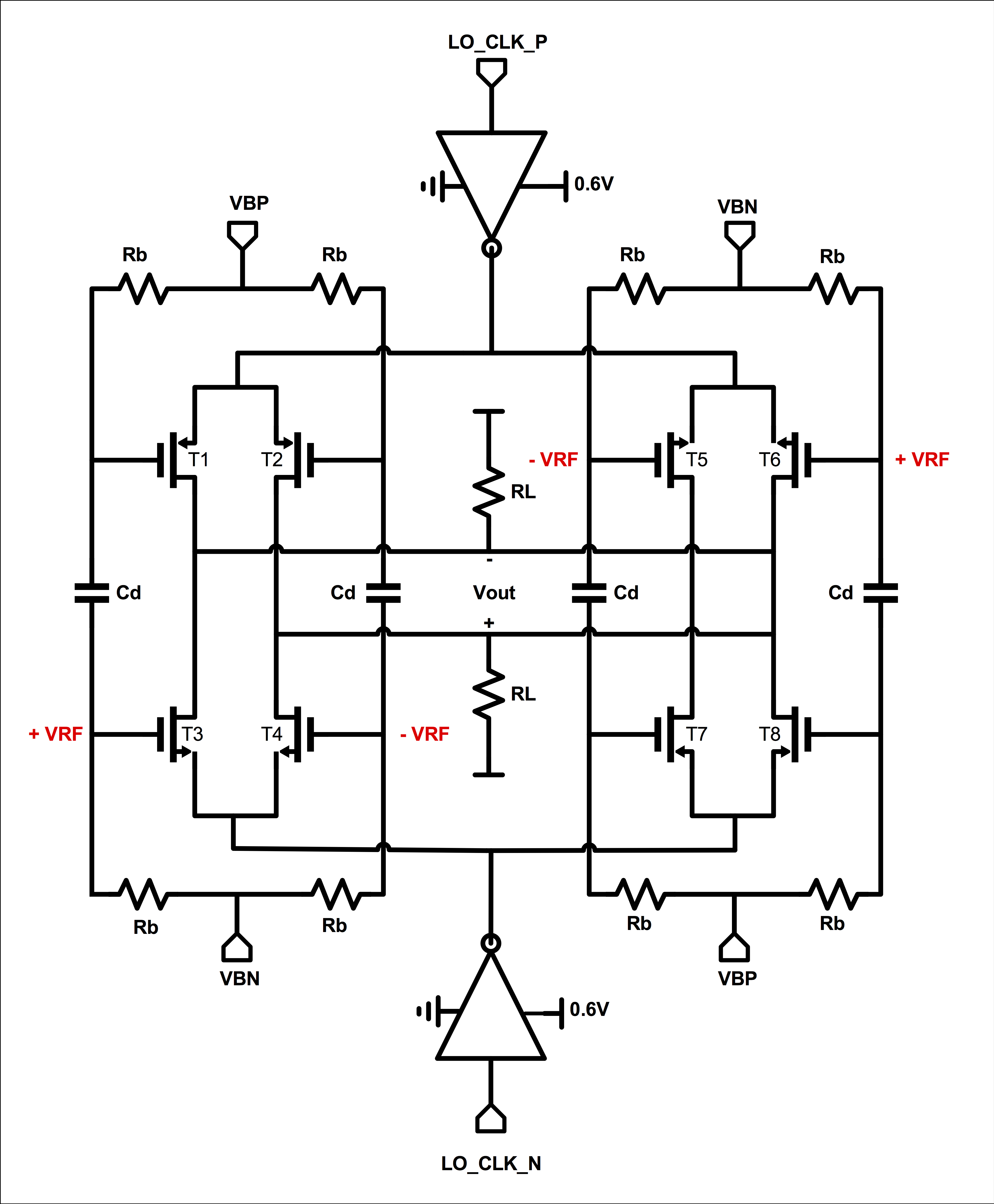
Fig.2 Simplified Schematic of Mixer
The conversion gain of the mixer can be expressed as
Circuit simulations show that the mixer has a conversion gain of 8dB, a single side-band noise figure of 20dB at an IF frequency of 10.7MHz. The LO clocks are generated using ideal voltage sources.
Differential-to-Single-Ended Converter
To interface with off-chip IF filters, a differential-to-single converter, shown in Fig.3, is used to convert the differential output signals of the mixer to a single-ended signal. It also acts as an output buffer to drive the filter.
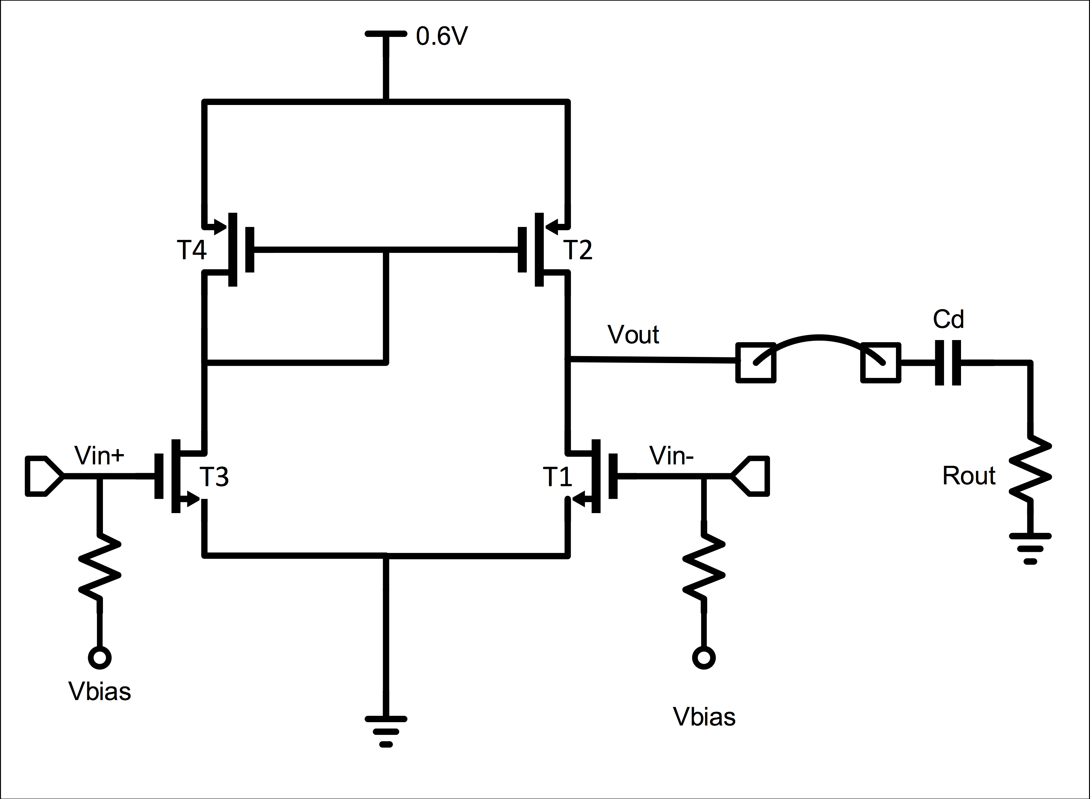
Fig.3 Simplified Schematic of Differential-to-Single-Ended Converter
The differential-to-single converter employs a simple "five-transistor OTA" structure without the tail current source. The tail current source is removed to save voltage headroom. Instead, T1 and T2 are biased separately to control their current consumption. Voltage gain of the differential-to-single converter is
Limiting Amplifier
A limiting amplifier is applied to rectify weak signals (as low as -60dBm) to rail-to-rail signals, which can be demodulated by backend circuits. Given a certain gain-bandwidth product (GBW), it's very hard to acquire both high gain and large bandwidth (BW). Therefore, multi-stage amplifiers, or cascaded structures, are employed as shown in Fig.4. The bandwidth of multi-stage amplifiers, , can be calculated from the bandwidth of each single stage, , with
Even though the limiting amplifier is used in open-loop, parasitic capacitance between input and output might cause feedback and hence oscillations. Post-layout simulations have been peformed to check the stability of the design. To minimize the DC offset, AC coupling is employed at each stage.
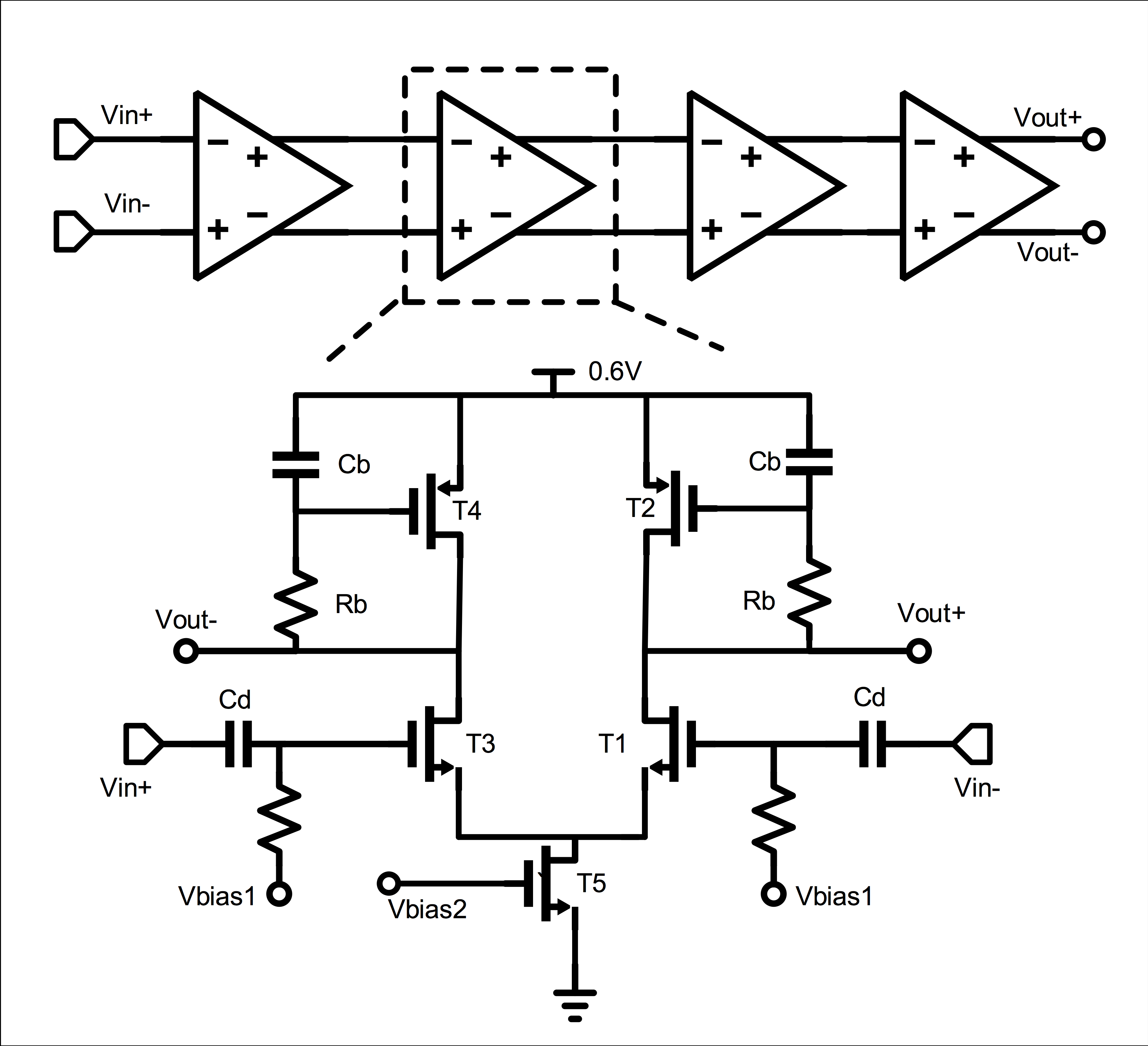
Fig.4 Simplified Schematic of Limiting Amplifier
T1 and T3, shown in Fig.4, form an input differential pair. T2, T4, Rb, and Cb form a complex load impedance. For DC signals, the circuit becomes a differential amplifier with diode-connected load, which results in low gain and a stable DC operating point. For AC signals, the complex load impedance is high at low frequency and is low at high frequency. Therefore, the complex load impedance can be considered as a low-pass filter. The simulated voltage gain from differential inputs to outputs of the limiter is around 73dB at the IF frequency of 10.7MHz.
Digital Demodulator
Based on the concept of narrow-band delta-sigma frequency-to-digital conversion [2], the digital FM demodulator, shown in Fig.5, contains two differential D-type flip-flops and a differential XOR gate. The demodulator converts rail-to-rail FM signals to a pulse-density modulated signal. The low-frequency audio signals can then be easily obtained by low pass filtering this signal using an LC low-pass filter after the demodulator.
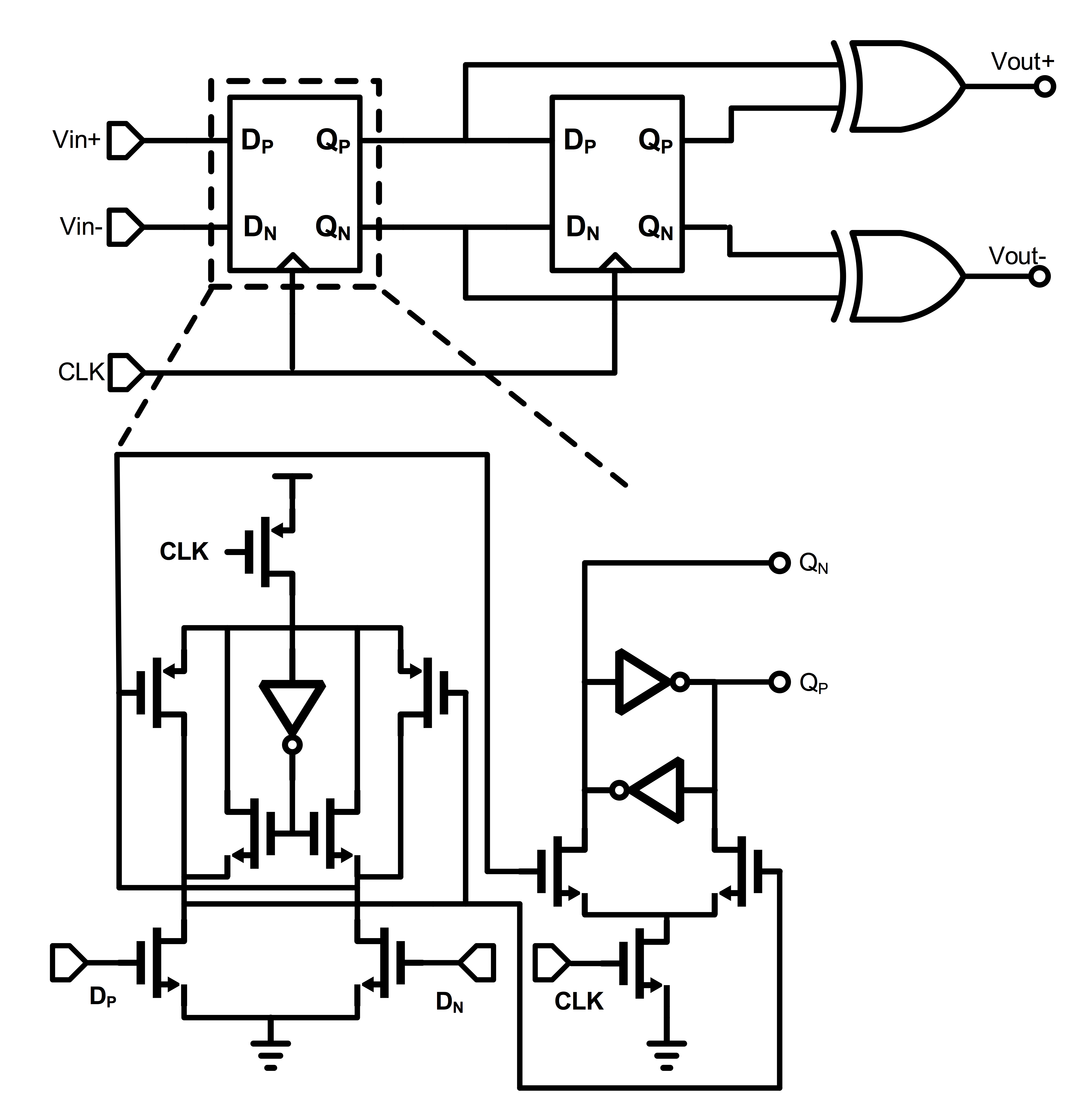
Fig.5 Simplified Schematic of Digital Demodulator
In simulation, a clock frequency from 2MHz to 3MHz can be used to demodulate FM signals with low distortion. Thanks to the all-digital structure of the demodulator, the power consumption is small, compared to that of the analog front-end. The theoretical signal-to-quantization noise ration (SQNR) of this demodulator is
,where is the maximum frequency of audio signal, is the demodulator clock frequency. is given by , where is the maximum deviation of FM signals. It is 150kHz in our case. Simulated voltage waveforms are shown in Fig.6. The upper graph shows the voltage waveform at the output of the digital FM demodulator. The output signal is a pulse-density modulated signal. When the frequency of the input signal is high, the output signal has a large DC component. When the frequency of the input signal is low, the output signal has a small DC component. After being filtered by an LC low-pass filter, the low-freqeuency audio signal is shown in the lower graph of Fig.6.
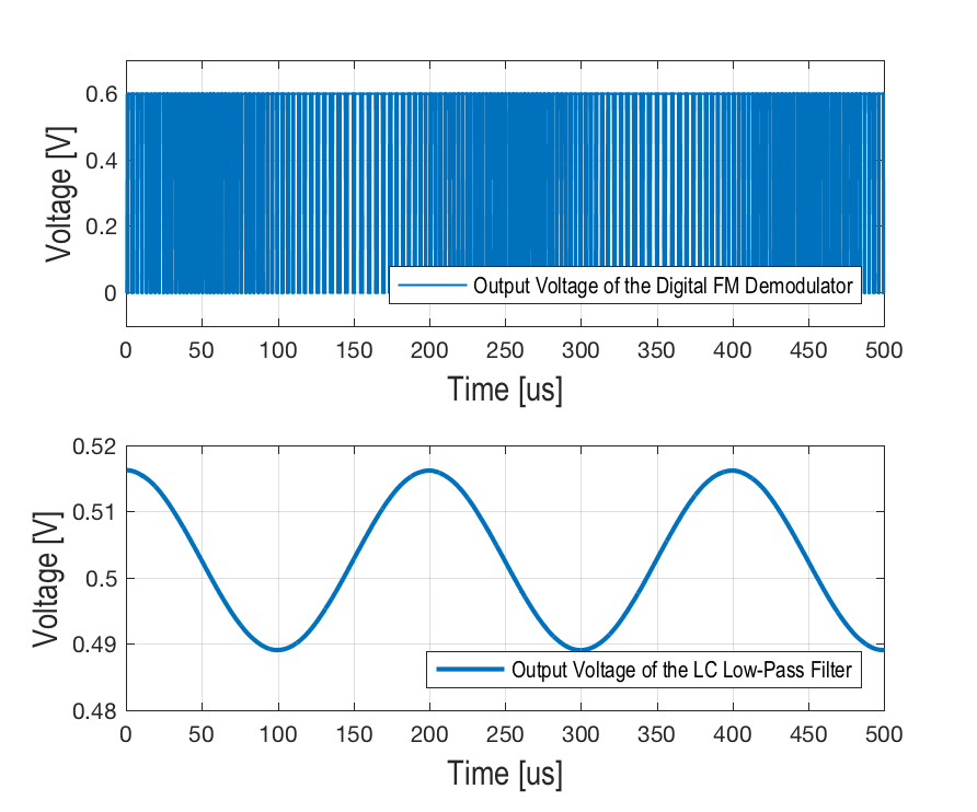
Fig.6 Output Voltage Waveform of Digital FM Demodulator and LC Low-Pass Filter